Welcome to the roadmap of innovation! In the realm of PCB development, every step is crucial. Join us as we unveil the essential journey from idea to reality. From schematics to assembly, we’ll guide you through the intricate process of crafting cutting-edge electronic designs. Let’s embark on this adventure together and unlock the secrets of PCB development in the UnioTech team.
What Software You Should Consider for PCB Creating?
Let’s explore the backbone of PCB production: the software. In this section, we’ll delve into top-notch options renowned for their versatility, functionality, and ease of use. Whether you’re a seasoned professional or an aspiring enthusiast, finding the right software is key to unlocking your PCB design potential. There are two most popular software for the PCB design:
- Altium Designer: Altium Designer is a comprehensive PCB design software known for its powerful features, intuitive interface, and advanced functionality. It offers a unified design environment for schematic capture, PCB layout, and component management, making it a top choice for professionals and enthusiasts alike.
- KiCad: KiCad is an open-source PCB design software that offers a range of features comparable to commercial alternatives. It provides schematic capture, PCB layout, and 3D visualization tools, along with a vibrant community and extensive library of components. KiCad’s affordability and flexibility make it a popular choice for hobbyists and small businesses.
9 Key Steps in PCB Development Flow
Now it’s time to discover the crucial step of PCB development. At UnioTech we followed 10 stages to create the PCBs with high quality and functionality.

Alt text: PCB Development Life Cycle
Step 1: Block Diagram is a Basic

Block Diagram
A block diagram is like a map showing how different device parts connect and work together. A block represents each part, and lines show how they’re connected. It’s crucial at this stage to picture and describe each device module.
Step 2: Calculations & Simulations

An Example of the PCB Simulation Process
Simulation is like a practice run for certain parts of the schematic that are supposed to work automatically using analog circuits. It’s like testing them in a virtual environment before building the real thing. This helps us ensure that these parts will behave correctly once the device is built. It’s a bit like trying out a recipe in a cooking simulation before making the actual dish – it helps us catch any mistakes or problems early on so we can fix them before they become bigger issues.
Step 3: Schematics Creation

PCB Schematics in Altium Designer
Schematics are like detailed blueprints that show a device’s electrical structure. At this stage, we take each block in the device’s structure and create a complete electrical schematic for it. Every module gets its own sheet of schematics, and they’re all connected in the main sheet.
The schematics for digital Integrated Circuits (ICs) and Microcontroller Units (MCUs) are based on the recommendations provided in the manufacturer’s data sheets and existing development boards. For analog and power circuits, we calculate their parameters using formulas and then simulate them using specialized software to ensure they’ll work as expected.
After completing this stage, a schematic document will be generated. We can prepare a preliminary Bill of Materials (BOM) and conduct a preliminary cost estimation.
Step 4: Footprinting and 3D Libraries

PCB Library Example
In modern PCB design, footprints and 3D libraries play a crucial role. PCB CAD software allows us to model PCBs in 3D, where every electronic component added in the schematics is represented by a 2D model showing soldering pads and the area it occupies, as well as a 3D model of the actual component. This means we can create a PCB layout that fits perfectly within the entire volume of the case or even design the enclosure around the 3D model of the PCB. This ensures that the final product is functional and fits seamlessly within its housing or casing.
Step 5: Placement Development


Example that Shows PCB Placement Stage
During the placement stage, we carefully position each component on the PCB, considering the recommendations provided by IC manufacturers for optimal performance. We aim to minimize the length of wires between elements, which helps reduce signal interference and improve the overall reliability of the PCB. Additionally, we pay attention to heat dissipation by strategically placing components to facilitate efficient cooling, which is particularly important for components prone to overheating. By the end of this stage, we’ll have a preliminary estimation of the PCB area needed to accommodate all components.
As a result, we obtain a preliminary 3D model of the printed circuit board, which allows us to perform preliminary calculations and integration with the mechanical part or enclosure.
Step 6: PCB Routing Stage

An Example of the PCB Routing Step
During the routing stage, we meticulously design the pathways, called traces, that connect the components on the PCB. These traces are made of copper and serve as conductive highways for electrical signals to travel between different parts of the circuit.
We consider various factors such as signal integrity, electromagnetic interference, and thermal management during routing. Properly routing the traces ensures that signals reach their destinations accurately and efficiently while minimizing the risk of interference and overheating.
In addition to creating the electrical connections, we generate a 3D assembly model of the PCB. This model visually represents how the components fit together in the final product, allowing us to verify clearances, assess mechanical constraints, and ensure compatibility with the enclosure or casing.
By completing the routing stage, we achieve a fully functional PCB design ready for manufacturing.
Afterwards, we conduct simulations of the completed board using various tools to ensure the system operates correctly.
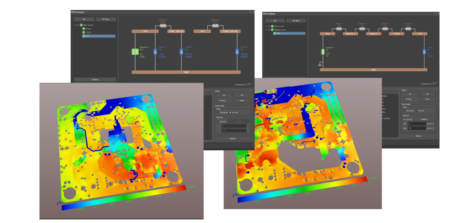
Completed PCB Simulations
Step 7: Production Files Export
We export production files from the CAD system to initiate the PCB manufacturing and assembly process. These files include all the necessary information for accurately fabricating and assembling the PCB.
Commonly exported production files include:
- Gerber files contain information about copper layers, solder masks, silkscreens, and drill data necessary for PCB fabrication.
- Bill of Materials (BOM): This document lists all the components required for the PCB assembly, including part numbers, descriptions, quantities, and reference designators.
- Pick and Place files: These files provide instructions for the automated assembly machines to place surface-mount components on the PCB accurately.
- Assembly drawings: Detailed drawings showing component placement and orientation on the PCB to guide the assembly process.
- A CAD project: refers to the digital design and documentation of a product or system using Computer-Aided Design (CAD) software.
- A PDF of schematics is a digital document that contains graphical representations of the electrical connections and components within a circuit. This document is typically generated from the CAD software used to design the schematics.
- PCB layer files are digital files containing information about each layer of a printed circuit board. These files are generated by CAD software during the PCB design process and are used for PCB fabrication.
By exporting these production files, we ensure that the PCB manufacturer and assembly service have all the necessary information to produce the PCB according to our design specifications.
Step 8: Production Support
Production support involves addressing any queries or requests from the PCB manufacturer during manufacturing. This may include providing additional drawings, clarifying part numbers, or resolving any issues that arise to ensure smooth production.
Efforts to support production typically involve:
- Prompt Response: Responding to manufacturer queries swiftly to minimize delays in the production timeline.
- Providing Additional Information: Furnishing any necessary supplementary drawings, specifications, or sketches to clarify design details or address manufacturing concerns.
- Clarifying Part Numbers: Offering clarification on part numbers or specifications to ensure accurate component selection and placement.
- Collaboration: Working closely with the manufacturer to troubleshoot and resolve any issues during the production process.
By providing comprehensive production support, we aim to maintain open communication and collaboration with the manufacturer. Ultimately ensuring the successful fabrication of the PCBs according to our design specifications.
Step 9: Bring-up Testing

Bring-up Testing of the Produces PCBs
Upon arriving at the assembled PCBs, we commence the bring-up tests to verify the board’s functionality. During this stage, we employ tools such as multimeters, oscilloscopes, logic analyzers, spectrum analyzers, and so on (all necessary equipment for checking the board) to examine various aspects of the PCB meticulously.
Specifically, our tests include:
- Supply Voltages: We measure all supply voltages to ensure they are within the specified ranges and free from fluctuations.
- Ripple Parameters: Using oscilloscopes, we assess the ripple parameters of power supplies to ensure stable and clean power delivery to components.
- Logic Functionality: We scrutinize the PCB’s digital buses and logic functionality using logic analyzers, confirming proper communication and signal integrity.
- Radio Part: Checking signal frequency and power, spectrum analysis. Assessing how well the antenna directs the signal in the required direction. Ensuring the device does not emit excessive interference and is resistant to external interference.
By conducting thorough bring-up tests, we can identify and rectify any issues early in the production process, ensuring that the PCBs meet performance requirements before proceeding to further testing or deployment.
Bonus: Our PCB Creation Principles
Well, there’s more. We’ve also prepared a little bonus for you! In this section, we provide information about the principles that guide us in the development of PCB.
It’s crucial to tailor the design when creating printed circuit boards (PCBs). You need to meet specific requirements based on the intended application. Here’s a breakdown of fundamental principles to consider for different PCB types.
When creating PCBs for mass production, our focus should be on the following key characteristics:
- Minimizing the PCB area as much as possible.
- Using the smallest number of layers.
- Choosing trace widths and VIA drill dimensions from standard capabilities.
- Using only through-hole VIAs, avoiding blind VIAs, VIA-in-pad technologies, and epoxy-filled VIAs.
- Avoiding immersion gold finishing.
- Optimizing the values listed in the Bill of Materials (BOM).
For PCBs designed for high-speed and RF applications, our priorities shift to:
- Routing RF traces and clearances based on impedance calculations and layer stackup.
- Ensuring differential line VIAs follow impedance calculations and layer stackup.
- Maintaining equal lengths for differential lines.
- Separating power on different layers and using polygons in layers.
- Keeping RF and high-speed lines separated from ground planes.
When developing high-power PCBs, our goals are to:
- Calculate power conducting trace and VIA sizes based on current ratings, copper thickness, and etching.
- Optionally reinforce power conducting VIAs with brass nails or fill them with tin.
- Simulate and test the final design using power distribution software.
In conclusion, mastering the essential steps of PCB development empowers you to transform ideas into reality with precision and efficiency. From schematic design to assembly, each phase plays a vital role in ensuring the success of your electronic creations. By understanding and implementing these steps effectively, you can confidently navigate the complexities of PCB development and achieve your desired outcomes.